Testing reports
This document describes all of the testing conducted on the QM of Amateur Payload. It includes testing procedures, testing results, testing conclusions and possible improvements for the FM design.
Test 1
Before powering on the Amateur Payload I discovered one major potential issue and one smaller one with the design.
Major issue
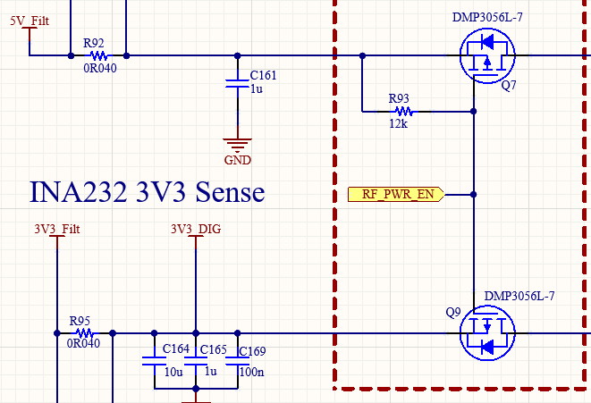
The RF_PWR_EN net is used for powering 3.3V and 5V RF part of the Amateur Payload. The RF_PWR_EN net is connected to a 3.3V tolerant GPIO pin. This pin controls two P-Channel Mosfets whose gates are pulled high to 5V (see picture below). And here is the issue. The MCU's pin is not 5V tolerant! Furthermore, even if it is 5V-tolerant, since the MCU turns on after 5V is present, it violates STM's requirement that the voltage of a 5V tolerant pin must always be < min(Vdd + 3.6V, 5.5V).
Minor issue
Some GPIO pins that connect to the gate of some MOSFETS are not pulled low/ high. This could lead to unintended switching during startup of the Amateur Payload.
Proposed fix for both issues:
- Fix for major issue:
- ADD N_MOS between RF_PWR_EN_NET and RF_PWR_EN
- Fix for minor issue:
- ADD pulldown to: RF_PWR_EN_NET, ANT_DEPL_1_NET, ANT_DEPL_2_NET, PA_EN_NET
- ADD pullup to: SW1_NET, SW2_NET, CANA_FAULT, CANB_FAULT
Test 2
The board is powered on and a blinky firmware is flashed onto the STM32. Voltages and current consumption will be measured on certain nodes
| Node | Voltage | Current |
|---|---|---|
| Vin | 5.00V | 106 mA |
| 3V3_DIG | 3.309V | ? |
Minor issue
The resistor for the status LED is only 38 Ohms. This means that the GPIO of the STM32 is sinking 8 mA.
Proposed fix
The resistor is replaced for a 200 Ohm resistor limiting current to approximately 3 mA.
Test 3
For the third test, we will turn on the PMOS's for the RF circuitry for a short period. The aim is to check the current consumption when the RF circuitry is in IDLE, meaning the analog part of the mixers is turned off and both PAs are also turned off. The expected power consumption is calculated in the table below:
| Component | Power (mW) |
|---|---|
| STM32 + DIG | 530 |
| 3 Mixers | 10 |
| LNA | 80 |
| IF AMPS | 360 |
| AGC | 130 |
| TOTAL | 1110 |
The expected current at 5V will be 222 mA.
The measured current at 5V, when RF circuit is enabled was 220 mA! So pretty close to our prediction.
Test 4
In this test, we check if Mixer 1, can be programmed and activated. We expect 266 mA. The measured current at 5V, when Mixer 1 is activated was 278 mA. So pretty close again to our prediction. We can also confirm that the mixer driver is reading out register values properly. So everything seems to work.
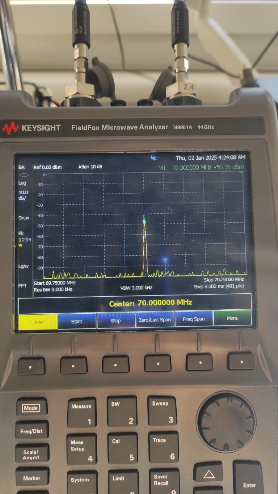
Test 5
In this test, we check if Mixer 1 outputs the expected IF frequency of 70 MHz, when feeding in a sinosoid at 436.065 MHz.
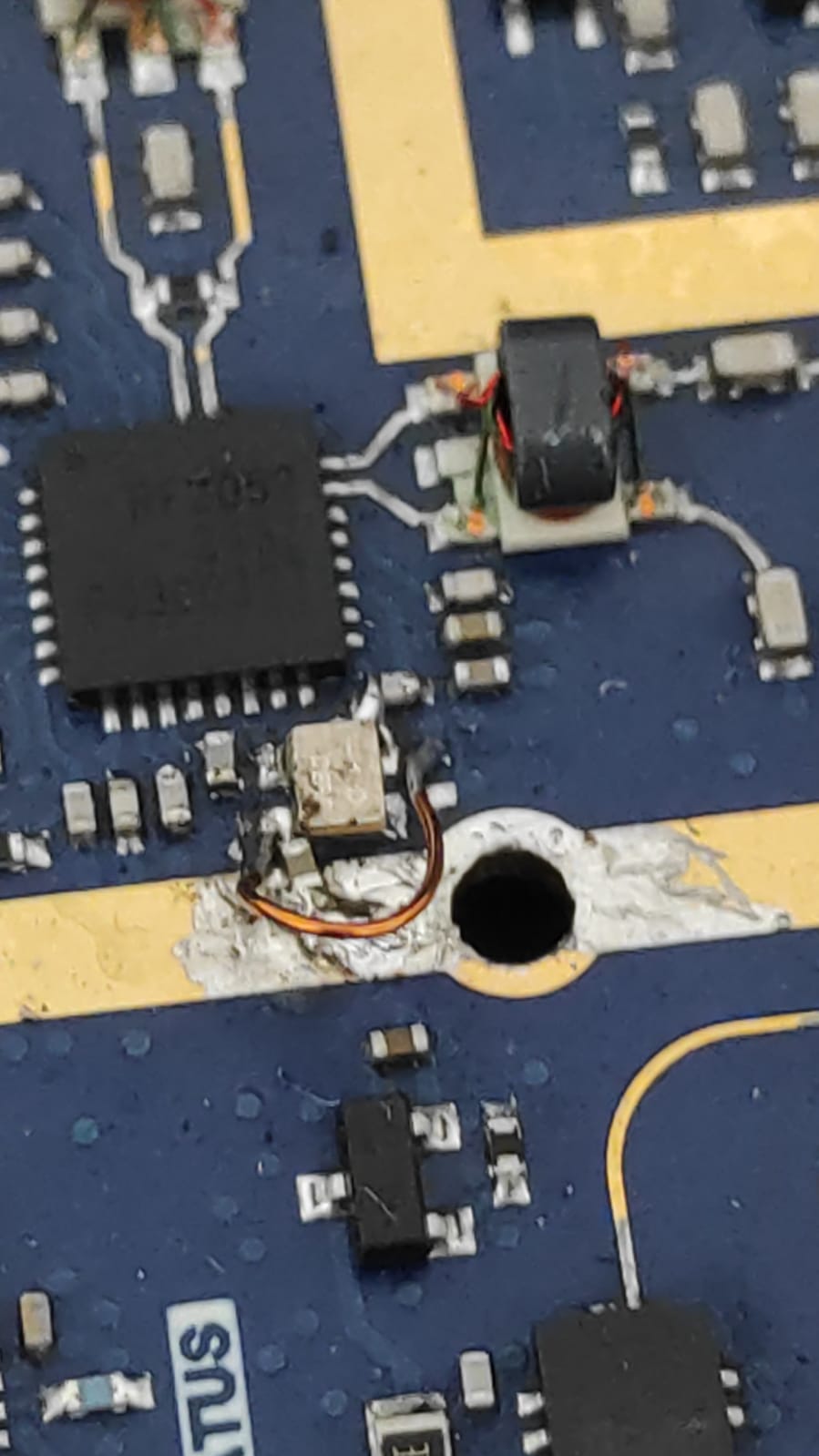
Major issue
After taking a look at the schematic, it was found that Vdd and Out were swapped with the TCXO.
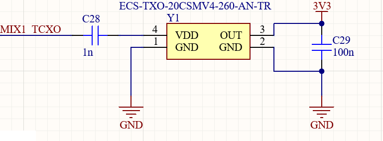
Fix for Major issue
Change the wiring, so that Vdd is connected to 3V3 and Out is connected to the input clock pin of the RF2052.
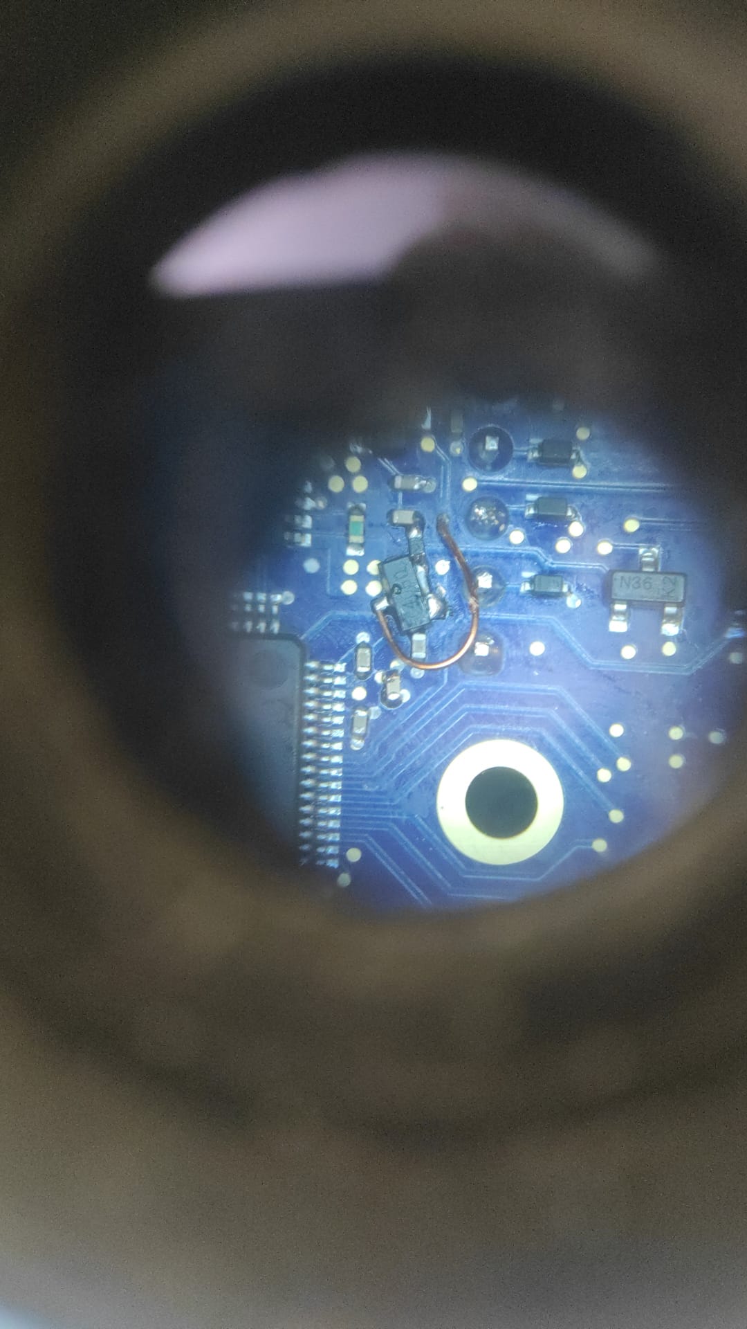
For the current board, the TCXOs were rotated by 90°, so that the connections were the right way around. The top right trace was cut and then connected to GND The bottom left trace was also cut and then connected to 3.3 V with a wire.
After modifying the TCXO circuitry, I performed a test by setting up the mixer the following way:
RF input centre frequency: 435 MHz (CW source selected at spectrum analyser) RF output centre frequency: 70 MHz LO setting: 365 MHz
After setting up the mixer, a clear peak at 70 Mhz could be observed. The measured power was -50 dBm, which is close to the calculated power (considering the used attenuator between input port of the AMPAY and the RF output port of the spectrum analyser). So all in all the test is successfull. One minor detail: The calibration of the mixer chip is only successfull if course tuning is disabled. This means that something is not quite correct when automatic tuning is selected. The hardware seems to be working fine. Current suspicion: driver issue.
Test 6
Test crystal filter and maybe adjust tuning
Test 7
Test VGA voltage settings and then test VGA
vgtest:
RefVoltage = 1.44 V
- 18-17 = -35 dBm, out = -5, gain = 30
- 18-12 = -30 dBm, out = -0.6, gain = 29.4
- 18-7 = -25 dBm, out = -0.6, gain = 24.4
- 18-2 = -20 dBm, out = -0.6, gain = 19.4
- 18+3 = -15 dBm, out = -0.6, gain = 14.4
Test 8
Test until after last mixer
Test 9
Test PAs
Test 10
Test complete RF chain