SatNOGS COMMS Hardware Version 0.3.2
This page explains how to work with the contents of the package from SatNOGS, where multiple breakout boards and cables were sent in addition to the SatNOGS COMMS v0.3.2. For a list of board components, scroll down to "Board components".
SatNOGS COMMS v0.3.2 and Friends
A short explanation of all components you will find in the SatNOGS COMMS package.
All info here is from the ICD, the User Manual (both available in the official repository), or experimentally determined by me (Pascal).
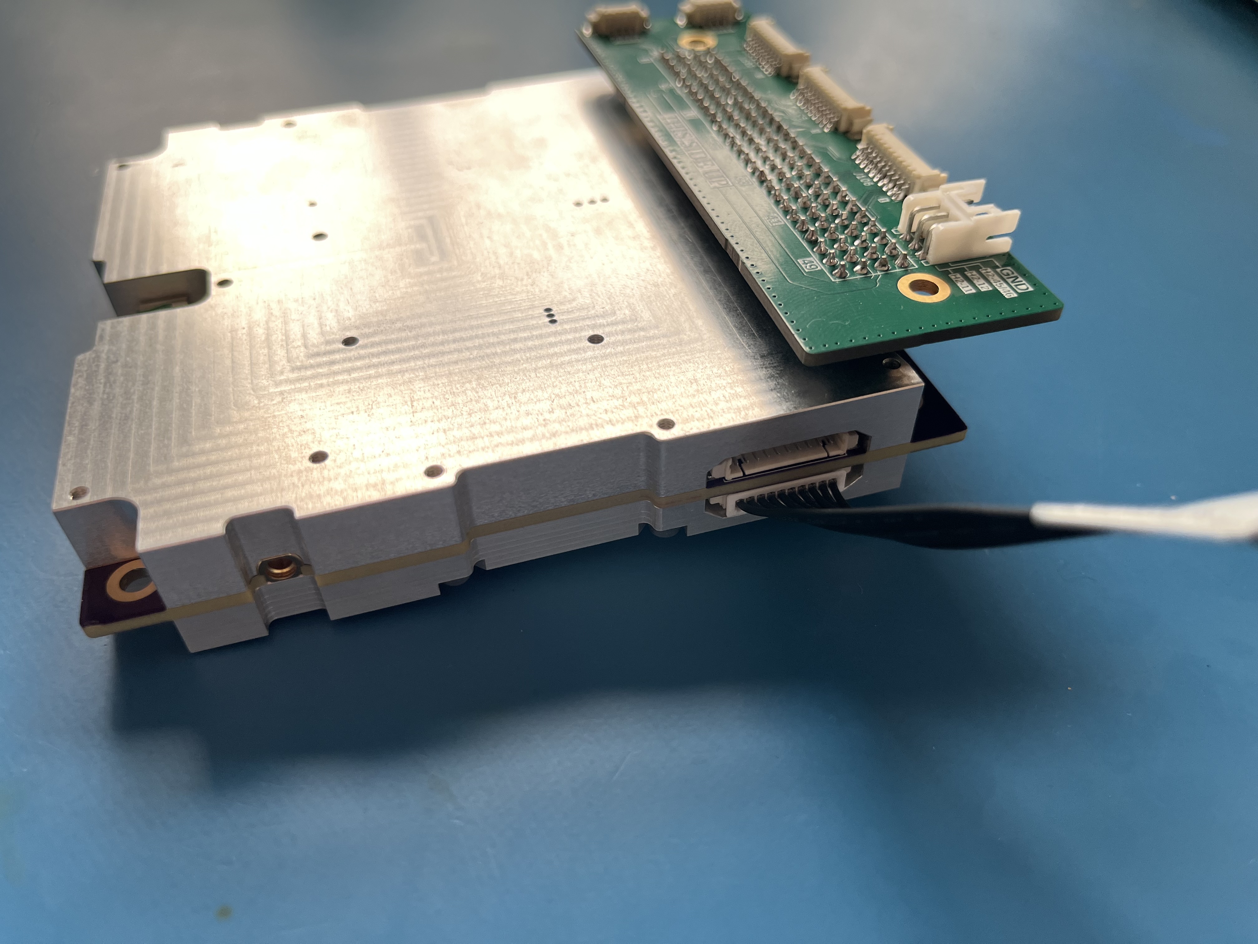
The board has flat 10 pin connectors (picoblade) for JTAG and SWD, FPGA and MCUconnectors that need to be connected via black 10 bus cables (picoblade) to a breakout board (J1 and J2).
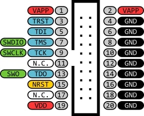
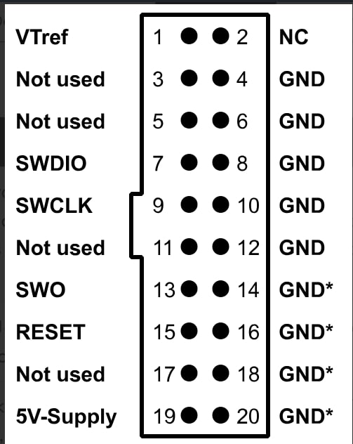
The two breakout boards are different: J1 has female headers and the whole “bottom” row of pins save for the one on the right are GND. the rest follows a specific assignment I have. As per User Manual, the J1 pins follow the assignment of a Segger J-Link EDU.
When looking into the female connector while the picoblade and jumper connectors sit on top of the J1 board, pins are top to bottom, then right to left 1-20 (derived from everything except 2 being GND).
J2 has male headers and contains 4 grounds, which fits the description of the FPGA JTAG connection.
the RF ports of the satnogs-comms are lodged into the board and i have no idea how to get to them to apply a 50R resistance (this needs to be done to ensure the device will not get broken when flashing)
The VGA-looking cable is actually a CAN bus cable with some pin assignments as specified in the user manual.
For the Banana Cable, the user manual shows a connection to the PC104 breakout boards with direct accesss to a certain pin selection to make powering the board simpler.
Doing things with the SatNOGS-COMMS v3.x
In the ICD document, the PC104 is explained (we will use a custom one on the flight version).
STLink PC and power connections
To connect the MCU to the ST-Link V2, the pinout of the STLink is given below first and the pinout of the breakout board can be derived from the Segger J-Link EDU second.
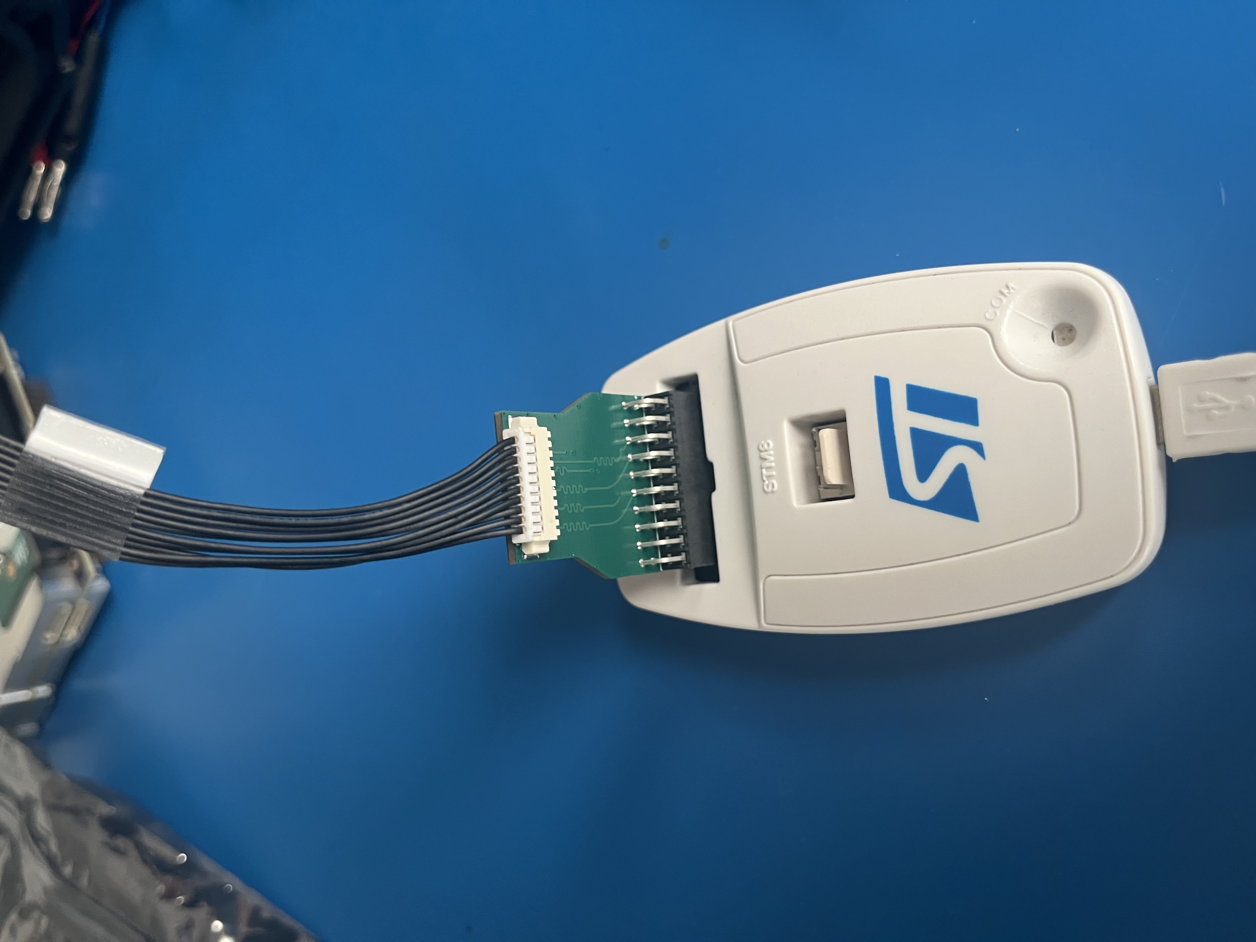
Connecting the MCU to a PC and a power supply, the required parts are shown first. Start by plugging in the J1 breakout board into the STLink as shown second.
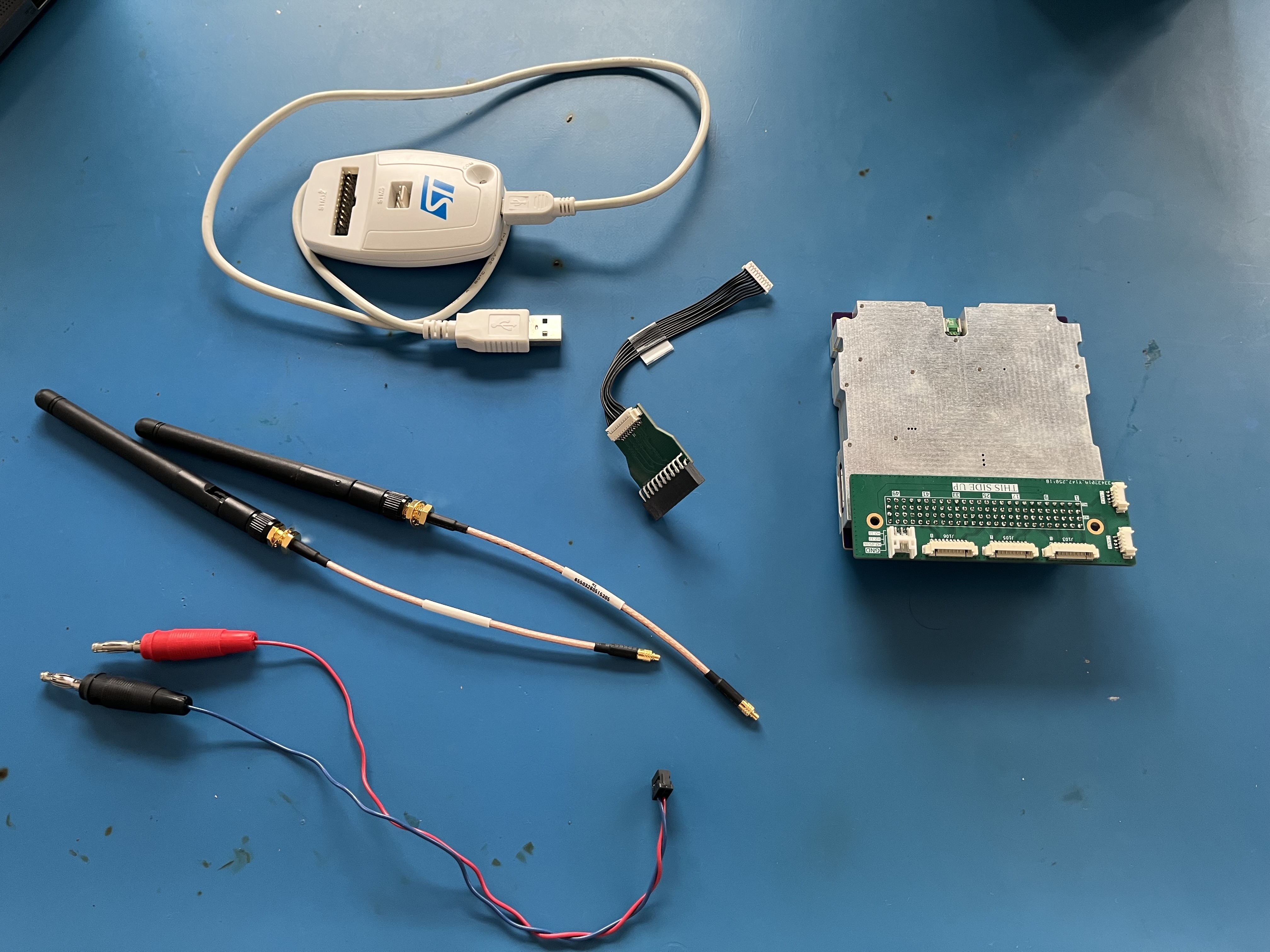
Next, plug the picoblade connector into the port that corresponds to the MCU, shown below first. To finalize the setup, plug the antenna RF cables into the ports on each side of the Satnogs-COMMS, and plug in the power connector to the PC104 breakout board. The board with all necessary connections will now look like the second one.


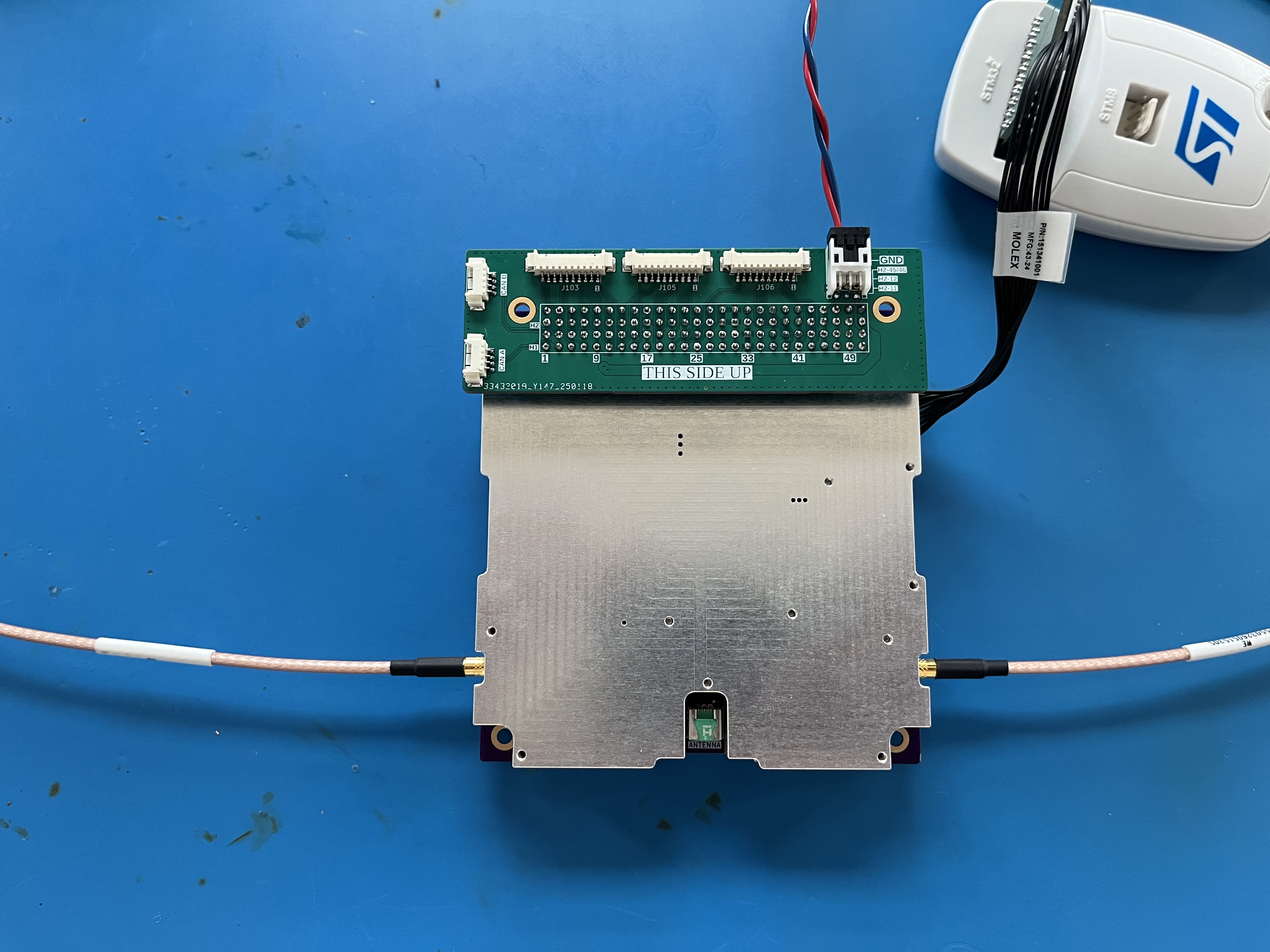
The USB cable of the STLink can now be plugged into the PC and the black and red banana cables can be plugged into a DC generator set to 12 V. Be sure to set a current limit at around 0.7 A!
CAN BUS connections
As described in the user manual document, the VGA looking cable can be plugged into the PC104 extension board to create a CAN bus interface. this has not been tested yet.
Board components
Control Library (satnogs-comms-software-mcu/libsatnogs-comms) Headers = Peripherals
ad8318: Demodulating Log Amp
CAN: 2x CAN bus transceivers
emc1702: Temp Sensor
F2972: single-pole double-throw (SP2T) reflective RF switch
FPF270x: current limit load switch
INA322x: Low Noise Diff Amp
LNA: Low Noise Amplifier
LP5912: Voltage Regulator
Radio: AT86RF215 Transceiver
RFFCX07x: RF Mixer (up/down conv)